요약
Through their continued collaboration, Imec and EV Group (EVG) are focusing on advancing the overlay performance required for advanced logic-to-logic and memory-to-logic tier stacking. Imec and EV Group (EVG) demonstrate a highly yielding wafer-to-wafer hybri…
본문
Through their continued collaboration, Imec and EV Group (EVG) are focusing on advancing the overlay performance required for advanced logic-to-logic and memory-to-logic tier stacking.
- Imec and EV Group (EVG) demonstrate a highly yielding wafer-to-wafer hybrid bonding technology at 200nm Cu interconnect pad pitch with record high post-bonding alignment accuracy, obtained on a test vehicle with routable interconnects.
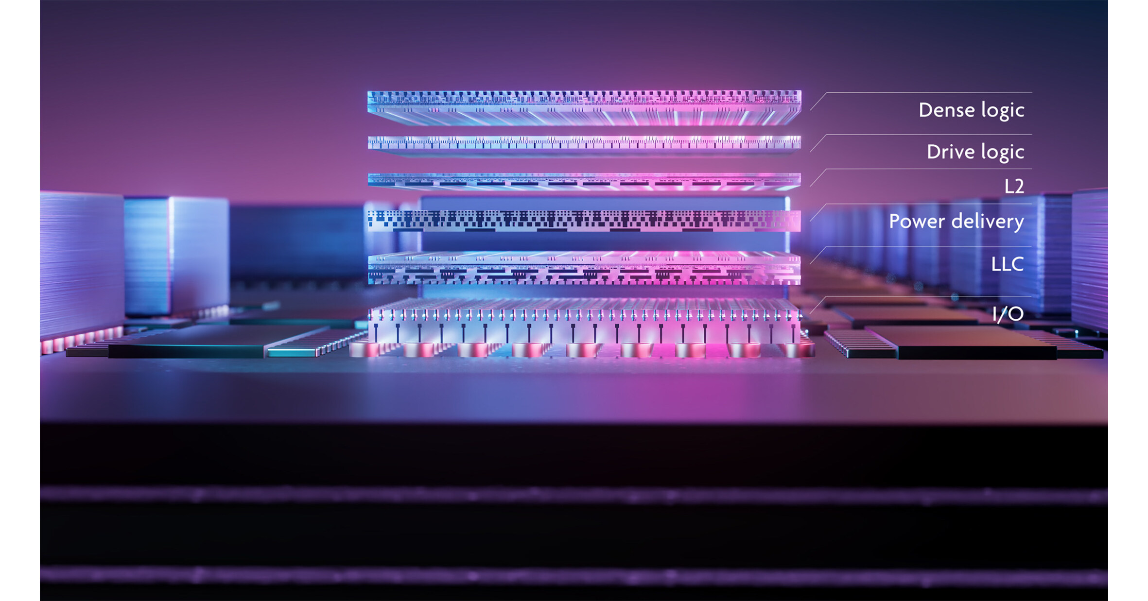
- This achievement marks a milestone in enabling advanced logic-to-logic and memory-to-logic tier stacking that requires an extremely high level of interconnect density – as envisioned in imec's CMOS 2.0 scaling paradigm.
- The breakthrough result was achieved by co-optimizing all critical elements of imec's wafer-to-wafer hybrid bonding process flow, and by leveraging EVG's most advanced wafer bonding equipment.
LEUVEN, Belgium, May 28, 2026 /PRNewswire/ -- This week, at the 2026 IEEE Electronic Components and Technology Conference (ECTC), imec, a world-leading research and innovation hub in advanced semiconductor technologies, and EV Group (EVG), leading provider of semiconductor manufacturing equipment and process solutions, present a robust and highly yielding wafer-to-wafer hybrid bonding technology at 200nm Cu interconnect pad pitch, demonstrated on a test vehicle with routable interconnects. In addition, a record high Cu pad alignment accuracy was achieved, leveraging EVG's most advanced wafer bonding equipment. Imec and EVG intend to further advance the wafer-to-wafer hybrid bonding roadmap, in support of logic-to-logic and memory-to-logic tier stacking use cases that require an extremely high level of interconnect density – as envisioned in imec's CMOS 2.0 scaling paradigm.
Continue Reading